

Analog Signal Modification Device
The Analog Signal Modification Device (ASMD ™) from Global Electronics, Ltd. simulates two types of soft faults from analog sensors: 1) drift in the sensitivity of the sensor, and 2) drift in the voltage associated with zero signal. Each of these perturbations can be activated individually or in conjunction with the other.
Although developed for use in automotive testing, the ASMD can be used in any system utilizing analog sensors whose output voltages vary linearly with the measured physical parameter (pressure, force, position, etc.), such as automotive sensors MAF, MAP, TP, etc†. By inserting this circuit between the output of the sensor and input to the measurement system (typically the A/D converter in the microcontroller), the sensor reading within the microcontroller will be intentionally skewed by the linear transformation of the ASMD:
OUTPUT = INPUT * GAIN + BIAS
where GAIN and BIAS settings of the ASMD are each independently adjustable over a range of values.
The ASMD contains three channels for simultaneously perturbing three signals with separate GAIN and BIAS of each (see Figure 1). Furthermore, each channel’s perturbation can be activated or bypassed (input fed directly to output) by a toggle switch on the panel (or activated remotely by logic-level control signals).
The typical use of ASMD is to test if the engine controller’s on-board diagnostic (OBD) can distinguish between the correct signal (bypass mode) and a degraded one (active mode) whose voltage lies within the sensor’s allowable range. Adjusting the BIAS or GAIN error allows detection thresholds to be determined.
The figure below depicts a simplified schematic of one channel of the ASMD inserted between the sensor and the input to the A/D measurement:
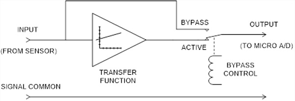
Because analog sensors sometimes utilize a signal common or return line separate from system ground to improve noise immunity, the ASMD includes an input for signal common (“Reference”) on each channel. This serves as the voltage reference for the INPUT and OUTPUT values in the preceding equation. Although signal returns are often near vehicle/battery ground potential, each reference on the ASMD may be independently driven several volts above/below vehicle/battery ground.
The figure below shows the input/output voltage traces for one channel with GAIN = 0.5 and BIAS = +1V.
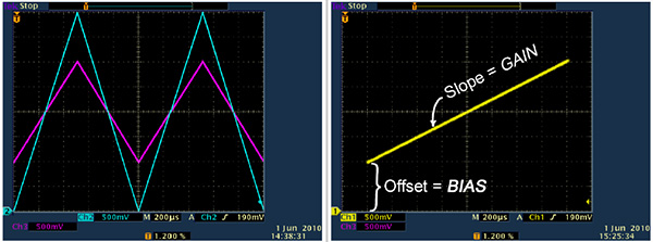
Left: Input (cyan) and Output (magenta) Right: Output versus input
†Sensors that encode analog readings as digital pulses for transmission to the controller are incompatible with ASMD.